The goal of this project is to reproduce an existing design for a hardware random number generator (RNG) implemented as a computer peripheral. The spirit is that of a lottery machine for which all relevant functional details are publicly verifiable, providing a basis for players' trust in its fairness.
Following from this, the functions of the RNG are broken down into two circuit board types which the customer can inspect and test in isolation and interchange at will. These are the "analog" board or noise source, which emits a stream of varying-width pulses, and the "digital" board or modulator which measures them against a quartz reference clock, and also regulates the power supply for the system.
We're starting with the analog board because it's the simplest in several respects: number and type of components, feasibility of hand-assembly for the initial prototyping or design validation stage, and software requirements (no chips to program).
There are no particular regulatory requirements for the manufacturing. There are a few strongly-desirables, to the extent they're economically feasible, especially considering the supply chain vulnerabilities in the industry which became common household knowledge in recent years:
- US based production process (though I expect Canada and Mexico would fit fine here too)
- No single-vendor components(i)
- No lead-free solder (that is, keep the traditional reasonable melting point)
- No mandatory "web application" for dealings with fab and/or assembly shop (as long as they can provide a human for us to talk to, what tools they use internally are of course up to them)
In general, what we're after is both a product and a process that are built to last.
Basic stats for the A-board:
- Dimensions: 3.0 x 4.2 cm
- Plain two-layer board, i.e. a single core with top and bottom copper layers
- All surface-mount components except for a right-angle 3-pin header, to be gold-plated at least in the production version
- All components and silkscreen printing on top
- Assorted vias with no particular size constraint
- A few larger vias with exposed annulus, serving as test points
- "Card holes" in the four corners to bolt it down, 3.5mm in diameter
- No further cutouts
Bill of materials, based on an early version,(ii) subject to revision:
| Qty | Description | Distributor | Dist. part # |
|---|---|---|---|
| 2 | Multilayer Ceramic Capacitor | Mouser | JMK212BJ476MG-T |
| 6 | Multilayer Ceramic Capacitor | Mouser | VJ0603Y104KXJCW1BC |
| 2 | Multilayer Ceramic Capacitor | Mouser | VJ0603Y103JXXPW1BC |
| 4 | Thick Film Resistor | Mouser | ERJ-3EKF1002V |
| 4 | Thick Film Resistor | Mouser | ERJ-3EKF2203V |
| 2 | Thick Film Resistor | Mouser | RK73H1JTTDD4700F |
| 4 | Thick Film Resistor | Mouser | CRCW060347K0FKEA |
| 1 | Header & Wire Housing 2.54MM BREAKAWAY RA 3 CKT Gold | Mouser | 22-28-8033 |
| 1 | 2-input XOR gate | Mouser | 74AUP1G86GW |
| 1 | EMI board-level shield | Mouser | BMIS-203-F |
| 1 | EMI board-level shield cover | Mouser | BMIS-203-C |
| 2 | Dual differential comparator | Mouser | LM393AM_Q |
The D-board is more uncertain and we'll work out the details when we get there, but as a starting point, its physical setup is largely the same as the A-board except for:
- Larger dimensions: 3.2 x 6.0 cm
- Rectangular cutouts of 1.0 x 0.4 cm on the short sides, making space for the A-board's thru-hole connector pins where it plugs in (the original design used two noise source boards to increase bit rate and redundancy)
We are currently soliciting manufacturing quotes and are open to different degrees of service: board fabrication only; assembly only, with customer-provided components; assembly with integrated component sourcing; fully integrated.
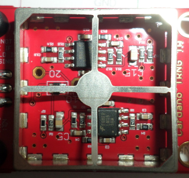
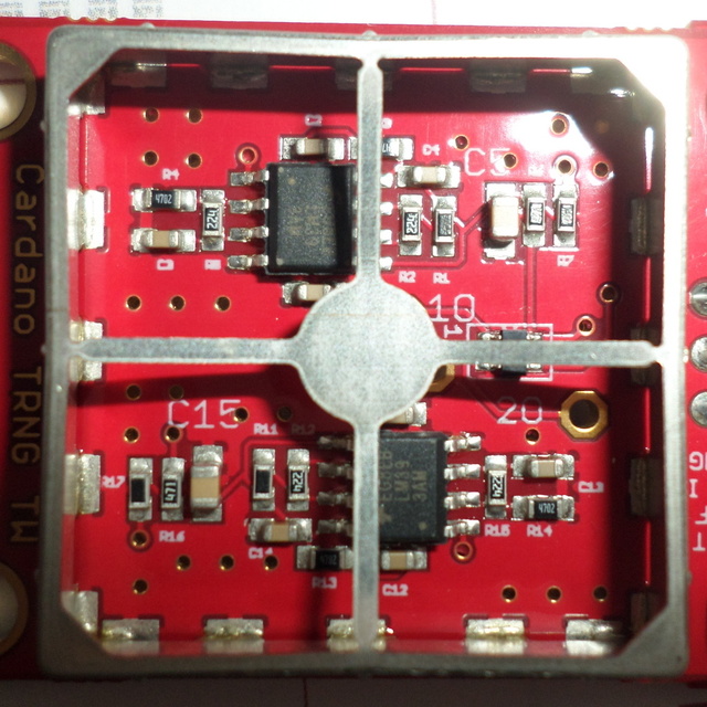
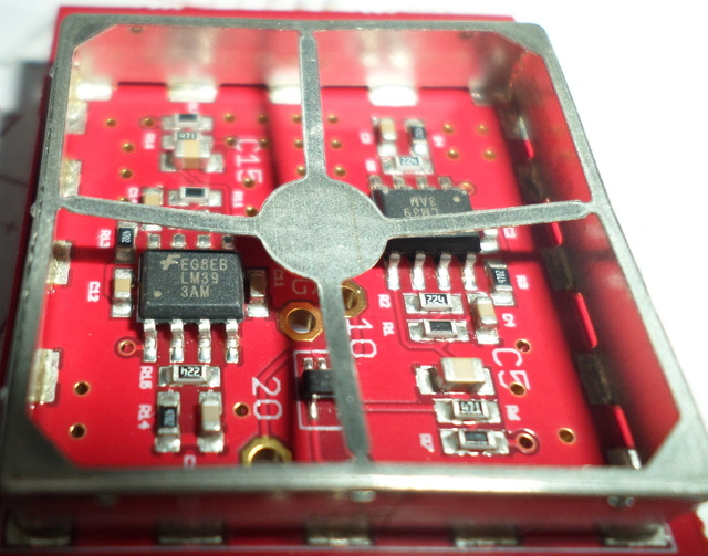
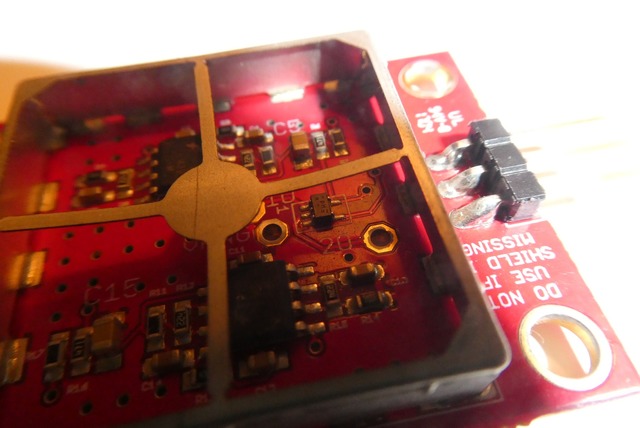
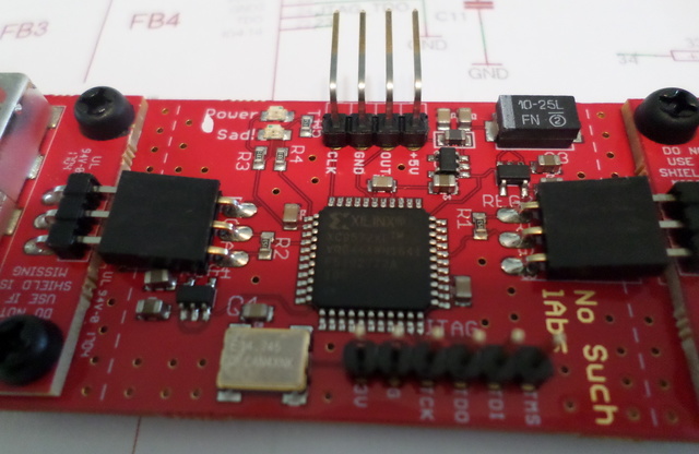
For some photographic aids from the original product, first the A-board:
The package markings on that XOR gate are particularly unhelpful, it's just "p H" and a couple horizontal lines. A well.
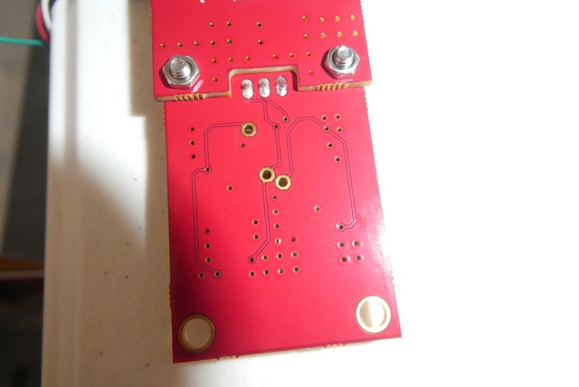
Test points and connector cutout:
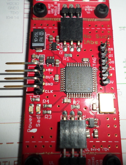
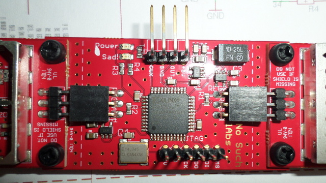
And the D-board. I have no idea why there's quite such a prolific scatter-shot on both boards of holes connecting the top and bottom grounding planes. Ten might not have been enough but a hundred would be just crazy?
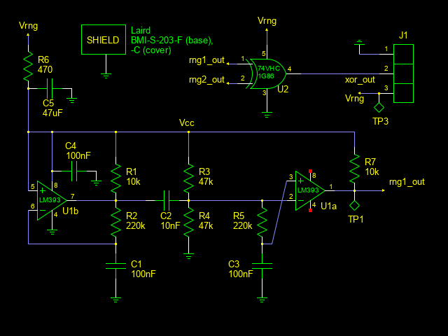
As a final teaser for those curious about our progress, here's a schematic that I've redrawn from the original almost unreadable "Eagle" output, rearranged somewhat to clarify (to my eye at least) the various functions and stages of the circuit.
Not pictured is the second identical instance of the main circuit, which accounts for the missing TP2 test point and rng2_out signal getting XORed with rng1_out (presumably doubling the bitrate).
As to that main circuit, I admit I don't yet fully understand why it's done the way it is, especially what the second comparator stage is doing and what considerations govern the particular choices of component values. My next step here will likely be to do some more in-depth probing of the internal signals on an existing board, trying out my Labrador to see if it's up to the task.(iii)
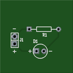
Finally, my "hello world" equivalent, an LED circuit in gEDA's "pcb". Besides this "artistic rendition" it of course also produces the vector outline graphics for each layer in gerber format.
- The modulator will likely use an FPGA, which squeaks by on the theory that the same HDL can be synthesized for different vendor stacks, albeit with considerable migration pain. [^]
- No updated BOM was published for the noise source, nor any at all for the modulator board, to my knowledge. [^]
- Docs say its oscilloscope mode can do 750k samples per second, and given that the final entropy output is only around 50kbps, frequency-domain intuition suggests it should be more than adequate to see the individual pulses and even the noise waveforms that trigger them. [^]
[...] of large unpredictable numbers aka entropy, and JWRD happens to have a small stockpile of hardware entropy devices, we naturally included one in the deal; but since they remain out of production we couldn't justify [...]
Pingback by Spreading entropy with rngnet, a first software edition « Fixpoint — 2024-01-29 @ 05:23
[...] and encrypted channels. I'd consider the crypto implementations suspect until proven otherwise, entropy sources especially, but perhaps no worse than cell phones generally, at least, or quite possibly better [...]
Pingback by First steps in long-range mesh networks: Meshtastic on LilyGo T-Deck Plus « Fixpoint — 2025-12-14 @ 22:52